VLSI Circuits–Oriented Gate-Length-Dependent DC–RF Compact Modeling of AlInN/AlN/GaN MISHEMTs with SSEC Extraction
DOI:
https://doi.org/10.31838/JVCS/07.02.02Keywords:
VLSI circuits, compactable model, gate length scaling, cut of frequency, small signal equivalent circuit, high frequencyAbstract
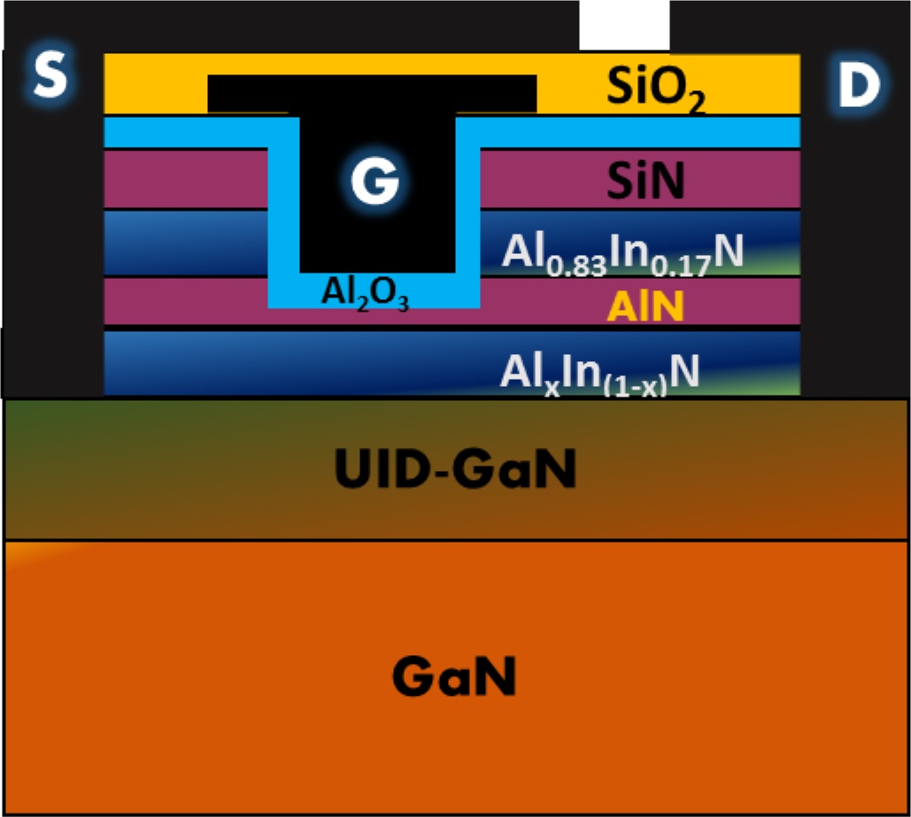
This work develops a compact analytical DC-RF model based on VLSI-circuit design that accounts for gate-length scaling impacts in RF circuit designs using . In order to effectively simulate the drain current density, transconductance and the gate charge for use in simulating RF and microwaves circuits using technology, a two-dimensional electron gas (2-D) sheet-charge based formulation has been developed to account for flat-band voltage and polarization charge impacts. This model was validated with both TCAD simulations and experimental data for a range of gate lengths (from 0.1 to 0.3 μm), resulting in a maximum drain current density of 2.35 A/mm and an estimated cut of frequency of125 GHz when the gate length was 0.1 μm. In addition, a refined small-signal equivalent circuit (SSEC) extraction methodology, integrating conventional and gradient-based optimization techniques, is introduced to improve parasitic de-embedding accuracy. Extracted S-parameters enable robust frequency-domain characterization, yielding fT=170 GHz and fmax=183 GHz. The proposed compact model demonstrates scalable, bias-consistent DC and RF prediction, making it well suited for VLSI RF and microwave circuit design and simulation using GaN MISHEMT technologies.
Published
How to Cite
Issue
Section