High Speed Energy Efficient Latch Architectures for Sequential Circuit Design
DOI:
https://doi.org/10.31838/jvcs/07.01.08Keywords:
latch, output noise, propagation delay, Power-delay -product, vlsi, D-Latch, Digital Circuit, RobustAbstract
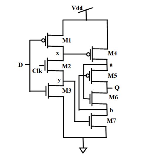
As per the escalating demand for portable and battery-powered electronic devices, the requirement of energy-efficient, high-speed devices with minimal area has become increasingly imperative in this era of sustainable electronics and green computing. Latches serve as fundamental elements essential for the operation of sequential circuits in Internet of Things (IoT), Edge computing, and high-performance processors. The bulk of on-chip elements in a processor is often composed of sequential parts such as memory, registers, counters and flip-flops, wherein the foundational component is a data latch. This research paper puts forward two level sensitive latch energy- efficient designs using 6 transistors and 5 transistors respectively. The proposed designs are assessed under multiple supply voltages and temperatures. Additionally, corner analysis and Monte Carlo analysis are conducted on the proposed latch designs to validate their robustness and stability, ensuring their sustainability and ability to withstand high error rate at different operating conditions. The results confirm reduced energy consumption, delay and output noise with improved performance of the latches with an improvement of PDP by 10 folds and the delay is reduced by a factor of 10-2 with an area occupancy of 5.6024 µm2 and 4.7183 µm2 for the two proposed designs. Also, a 3-bit shift register is designed with the proposed design to demonstrate the successful application of these designs.
Downloads
Published
How to Cite
Issue
Section