A 3.7-4.8GHz Programmable Integer-N PLL With Multi-Modulus Divider and Tunable VCO in Standard 45nm CMOS Technology
DOI:
https://doi.org/10.31838/jvcs/07.01.10Keywords:
Phase Lock Loop, , Programmable VCO,, programmable frequency divider, , source switched charge pump,, three state phase frequency detectors.Abstract
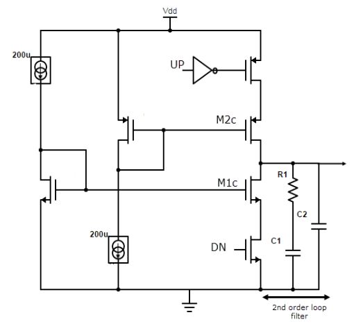
This paper presents a comprehensive study of each phase-locked loop (PLL) component to enhance its flexibility for various applications. First, a differential voltage-controlled oscillator (VCO) is designed with programmability enabled through a capacitor bank controlled by a 4-bit word, allowing it to cover a wide frequency range. Second, an integer- type frequency divider is implemented using a multi-modulus technique, introducing programmability to the divider. The multi-modulus divider consists of seven divider stages, where each stage can divide the input frequency by a factor of two or three, controlled by a seven-bit control word, enabling a wide range of division values. Since the frequency decreases after each stage, each divider stage is optimized for power efficiency. Third, a phase-frequency detector is designed with an extended phase detection range from
-2π to +2π. Additionally, a charge pump and loop filter are designed to provide a stable control voltage, ensuring the VCO operates at the desired frequency. The PLL is designed using the Cadence Virtuoso Analog Design Environment with 45nm CMOS technology and simulated using the Spectre simulator. Operating at a 1.1V supply, the PLL achieves a lock state in 14μs while consuming 27.4mW of power. The designed PLL delivers stable output frequencies in the range of 3.7–4.8GHz. The PLL shows PSRR of about 8dB when a small AC noise source (Vn=1mV) applied on the power supply.