A Novel Investigation on p-GaN GATE with and without AlGaN Back Barrier for AlGaN/GaN High Electron Mobility Transistors
DOI:
https://doi.org/10.31838/JVCS/07.01.18Keywords:
p-GaN Gate, Back Barrier, Silicon Carbide Transconductance, Threshold Voltage, E-mode, Ambient TemperatureAbstract
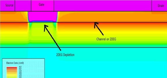
p- GaN layers is relatively matured and controllable, making p-GaN HEMTs the leading structure that is most likely to be commercialized. The analysis of the gate design parameters like transconductance, breakdown voltage, threshold voltage, JFOM and gate turn-on current of p-GaN devices, which determine the on-state characteristics, needs to be investigated. The AlGaN barrier, p-GaN gate, GaN, AlGaN back barrier, and SiC substrate constitute the structure of p-GAN, which is operated in the E-mode. The use of AlGaN back barrier reduces the punch-through current. Silicon Carbide (SiC) is used as substrate to have lower lattice mismatch with nitride layer. The transfer characteristics, transconductance, threshold voltage, breakdown voltage and JFOM are analyzed. The device demonstrates a positive threshold voltage that varies linearly with changes in ambient temperature. Additionally, the device featuring an AlGaN back barrier shows a higher breakdown voltage of 105V, in contrast to the device lacking a back barrier.
Published
How to Cite
Issue
Section