Energy Efficient and Radiation Hardening Dual Interlocked SRAM Cell Design Using Alternate Technology
DOI:
https://doi.org/10.31838/JVCS/07.01.24Keywords:
SRAM, Radiation Hardening, Low Power, CMOS, FinFETAbstract
Sources of radiation are packaging and environment. Heavy irons, alpha and protons constitute the radiation sources. In this problem, alpha particles are majorly involved due to packaging materials of the circuits in the chip. Protons are due to dopants used in semiconductors. Indirect ionization causes this event. The particles interact with electrons and produce the charge deposition processes. The charge collection alters the functioning of the circuit nodes. Reliability of memories are affected by the particle radiation which are responsible for Single Event Upsets (SEUs). The CMOS technology is prone to SEUs when fabricated for SRAM chips which store information. The other problem is single event multiple-node upsets. The circuit to be designed should have radiation hardening features.
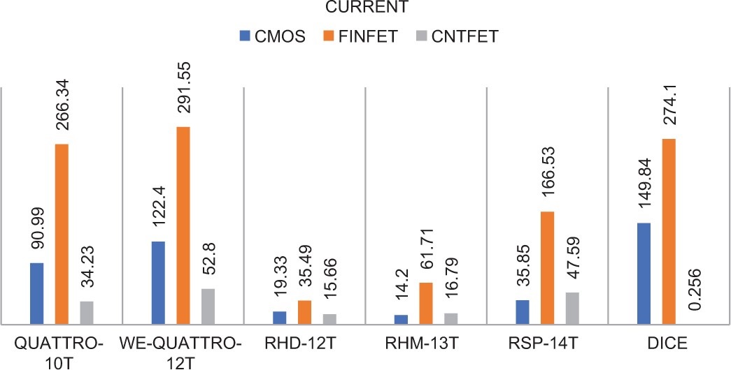
In this work different configuration based on negative feedback restoration of logic based SRAM design, multinode structure with radiation suppression, storage node with pull up NMOS transistor, multi-node upset elimination circuit, . radiation hardened circuits were designed and implemented. A dual interlocked storage cell SRAM is proposed which has higher radiation tolerance. the percentage of error occurrence is less compared to the conventional circuit. The configuration provides better driving capability for increased word line.The circuits were implemented in CMOS, FinFET and CNTFET devices. Silicon on Insulation (SOI) substrates will reduce this effect and FinFET devices will eliminate the further problems in CMOS. But the results shows that the Carbon nanotubes perform better in power and delay when compared to FinFET and CMOS.